**The ADG788BCP: A Comprehensive Technical Overview of Analog Devices' Low-Voltage CMOS Dual SPDT Switch**
In the realm of analog signal routing and switching, precision, reliability, and low power consumption are paramount. Analog Devices' **ADG788BCP** stands as a quintessential solution, embodying these critical characteristics in a compact, high-performance package. This integrated circuit is a **monolithic, CMOS-based dual single-pole/double-throw (SPDT) switch** designed to operate seamlessly in low-voltage applications, making it an indispensable component across a wide array of electronic systems.
**Core Architecture and Functionality**
The ADG788BCP integrates two independently controllable SPDT switches on a single chip. Each switch is configured with a common input (COM) and two outputs (NO – normally open, and NC – normally closed). The state of each switch is determined by the logic levels applied to its individual control pin (e.g., IN1 for Switch 1, IN2 for Switch 2). A fundamental strength of this design is its **low-voltage operation, supporting supplies from +1.8 V to +5.5 V**. This wide range ensures compatibility with modern microcontrollers, DSPs, and other digital systems that frequently operate at 1.8V, 3.3V, or 5V logic levels, eliminating the need for cumbersome level-shifting circuitry.
**Key Performance Characteristics**
The device's performance is defined by several standout specifications that make it suitable for precision applications.
* **Low On-Resistance (Ron):** The switch boasts a very low on-resistance of typically **4.5 Ω**, which remains exceptionally flat across the entire signal range. This is crucial for minimizing signal attenuation and distortion, especially when switching low-level analog signals.
* **High Bandwidth:** With a -3 dB bandwidth exceeding 200 MHz, the ADG788BCP is capable of handling **high-speed signals**, making it suitable for video routing, RF signal switching, and fast data acquisition systems.
* **Ultra-Low Power Consumption:** Built on an advanced CMOS process, the device features **minimal static power consumption** (leakage currents in the nA range). This makes it ideal for battery-powered and portable equipment where power efficiency is critical.

* **Excellent Linear Performance:** The switch exhibits low total harmonic distortion (THD) and high off-isolation. This ensures that the **signal integrity is preserved** with minimal crosstalk between channels when the switch is in the off state, which is vital for audio and measurement applications.
**Applications and Use Cases**
The combination of its dual-switch design and robust electrical characteristics opens the door to numerous applications. It is commonly employed in:
* **Battery-Operated Equipment:** For signal routing in smartphones, tablets, and medical monitors.
* **Audio and Video Signal Routing:** Switching between different audio sources or video channels.
* **Communication Systems:** Antenna and signal path switching.
* **Automated Test Equipment (ATE) and Data Acquisition Systems:** Multiplexing analog signals from sensors to an ADC.
**Package and Integration**
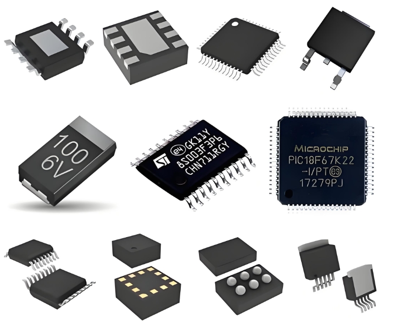
The "CP" in the part number denotes a 10-lead LFCSP (Lead Frame Chip Scale Package). This package offers a significantly reduced footprint and excellent thermal performance, which is essential for space-constrained PCB designs.
**ICGOODFIND Summary:** The **ADG788BCP from Analog Devices** is a highly integrated, **low-voltage, dual SPDT analog switch** that excels in performance and efficiency. Its **low on-resistance, high bandwidth, and minimal power consumption** make it a superior choice for designers who need reliable and precise signal switching in modern portable and high-speed electronic systems.
**Keywords:** Low-Voltage CMOS, Dual SPDT Switch, Low On-Resistance, High Bandwidth, Signal Integrity.
