NXP 74LVC1G11GV: A Comprehensive Technical Overview of the Single 3-Input AND Gate
In the realm of modern digital design, the demand for miniaturization and efficient use of board space is ever-increasing. The NXP 74LVC1G11GV addresses this need perfectly as a single 3-input AND gate in an ultra-small package. This device represents a crucial component in logic function implementation, offering a blend of high performance, low power consumption, and exceptional versatility for a wide array of applications.
As a member of NXP Semiconductors' renowned 74LVC family, this gate is built with advanced CMOS technology, ensuring low-voltage operation and compatibility with a broad spectrum of logic levels. The 'G' in its nomenclature signifies its status as a single gate, part of a growing class of monofunctional logic ICs that optimize PCB layout and reduce overall system size.
Key Technical Specifications and Features
The 74LVC1G11GV is designed to operate with a wide supply voltage range, from 1.65 V to 5.5 V. This makes it exceptionally versatile, capable of interfacing seamlessly with both older 5V systems and modern microcontrollers and processors running at 3.3V, 2.5V, or even lower voltages. Its core function is to perform the logical AND operation, where the output Y becomes HIGH only if all three inputs (A, B, and C) are HIGH.
A standout feature of this IC is its very low power consumption, a direct benefit of its CMOS architecture. This makes it an ideal choice for battery-powered and portable devices where energy efficiency is paramount. Furthermore, it boasts high noise immunity, a critical characteristic for maintaining signal integrity in electrically noisy environments.
The device incorporates overvoltage tolerant inputs up to 5.5V, regardless of the supply voltage. This means that even if the chip is powered by 1.8V, it can safely accept input signals from a 3.3V or 5V logic device without risking damage, eliminating the need for external level-shifting components.
The output stage features a balanced drive strength (±32 mA at 3.0V VCC), providing strong output current capability for driving multiple inputs or transmission lines while minimizing switching noise. The chip is also specified for live insertion capability, supporting hot-plugging applications.
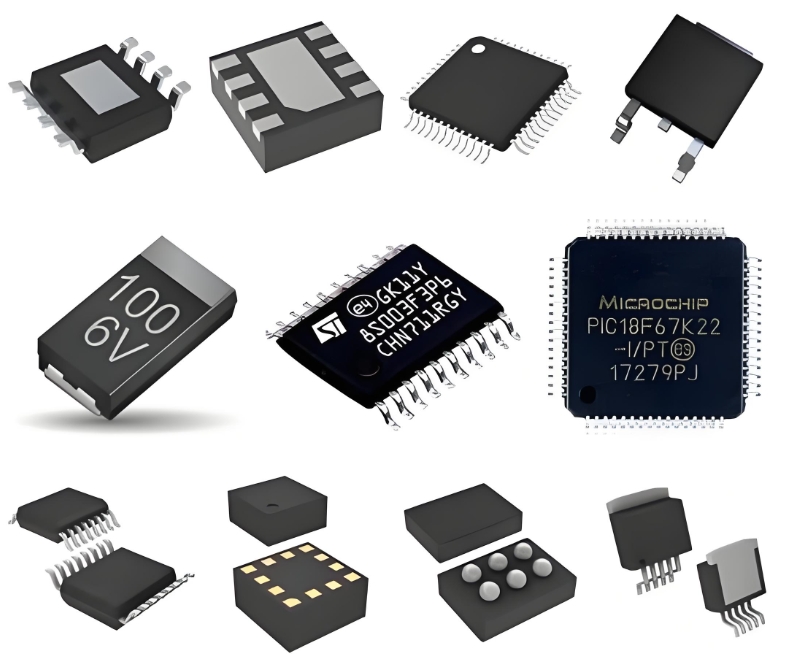
Housed in the tiny SOT753 (or SC-74A) package, the 74LVC1G11GV is the embodiment of space-saving design. This minuscule footprint is invaluable in densely populated PCBs found in consumer electronics, IoT sensors, and communication modules.
Typical Applications
The utility of a single 3-input AND gate is vast. It is commonly used for:
Gating and Enable Functions: Controlling the passage of a signal only when three separate enable conditions are met.
Address Decoding: In simple memory or peripheral select circuits where multiple address lines must be HIGH.
Data Validation: Ensuring multiple control signals are present before a data transaction is approved.
Waveform Generation: Creating specific output pulses based on the combination of three input clock or signal lines.
System Power Management: Combining multiple "good" signals (e.g., "Power Good," "Reset Released," "Clock Stable") to generate a master system enable signal.
ICGOODFIND Summary
The NXP 74LVC1G11GV is a highly integrated, versatile, and efficient solution for implementing a fundamental 3-input AND logic function. Its combination of a wide voltage range, ultra-small package, robust I/O protection, and low power consumption makes it an exceptional choice for designers aiming to enhance density and performance in modern digital systems, from portable gadgets to complex industrial controllers.
Keywords:
1. Single 3-Input AND Gate
2. Low-Voltage CMOS (LVC)
3. Wide Supply Voltage Range (1.65V - 5.5V)
4. Overvoltage Tolerant Inputs
5. Space-Saving SOT753 Package